Chemical Vapor Deposition (CVD)
Chemical vapor deposition (CVD) is a vacuum deposition method used to produce high-quality, and high-performance, solid materials.
The process is often used in the semiconductor industry to produce thin films.
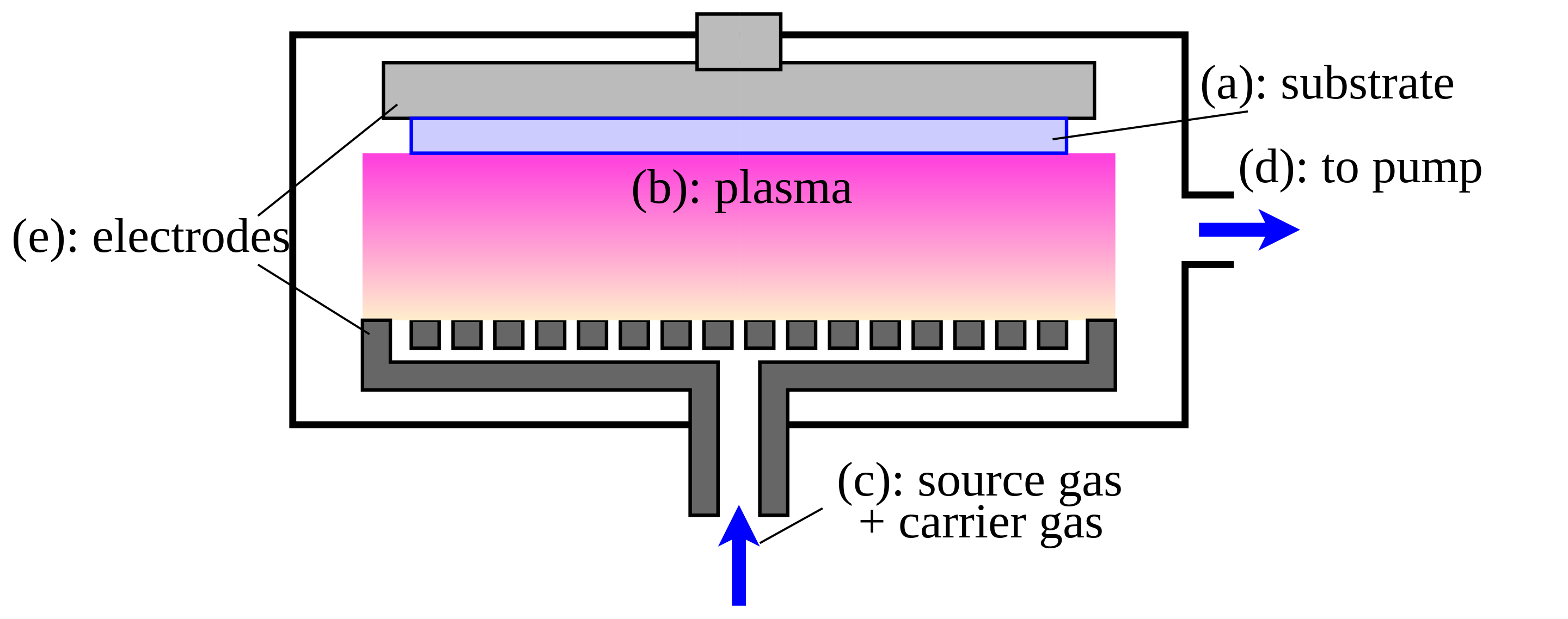
In typical CVD, the wafer (substrate) is exposed to one or more volatile precursors, which react and/or decompose on the substrate surface to produce the desired deposit.
Frequently, volatile by-products are also produced, which are removed by gas flow through the reaction chamber.
Microfabrication processes widely use CVD to deposit materials in various forms, including: monocrystalline, polycrystalline, amorphous solid (non-crystalline solid), and epitaxial.
These materials include: silicon (Si) (dioxide, carbide, nitride, oxynitride), carbon (C) (fiber, nanofibers, nanotubes, diamond and graphene), fluorocarbons, filaments, tungsten, titanium nitride (TiN) and various high-κ dielectrics.
The term chemical vapor deposition was coined 1960 by John M. Blocher, Jr. who intended to differentiate chemical from physical vapor deposition (PVD)
Plasma assisted CVD